Innovations at the nano scale
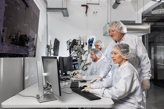
Innovative miniaturised systems are developed in the Technology Laboratory for Nano and Microsystems (TNM).
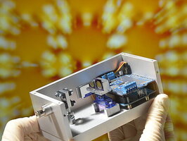
Nano and microsystems combine mechanical, optical, biological and electrical elements to realise innovative functions for sensors and actuators. These systems are of crucial importance in medicine, energy supply and materials science.
Students, employees and doctoral candidates can acquire practical knowledge in the laboratory and apply their knowledge in current research projects. Access to state-of-the-art technology and current research topics qualifies them for promising careers in a wide range of industries.
We work closely with companies and other research institutions in joint projects. Examples of our research activities can be found under the Internal link opens in the same window:Institute for Microsystems Technology.
Responsibilities and services for students
The Technology Laboratory for Nano and Microsystems offers a wide range of opportunities for students, doctoral candidates and researchers. Here, students in the Internal link opens in the same window:Smart Systems and Internal link opens in the same window:Micromedical Engineering degree programmes can acquire basic skills in microsystems technology and characterisation in the clean room in various internships, and deepen their knowledge in assistant positions and theses.
Exciting opportunities open up after graduation − in third-party funded research projects, graduates can participate directly in innovative research and development processes as project collaborators. Many take the opportunity to do a doctorate at our university and thus lay the foundations for a successful academic career, as our university can award doctorates. Click here for more information about the Internal link opens in the same window:HFU doctoral programme.
Together with the Internal link opens in the same window:Rottweil Research Center, we form the Internal link opens in the same window:Institute for Microsystems Technology (iMST).
Areas of specialisation
- Sensors and actuators (micro-electro-mechanical systems, MEMS)
- Optical systems (Micro-Opto-Electro-Mechanical Systems, MOEMS)
- Electrochemical etching processes / anodization
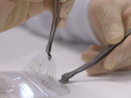
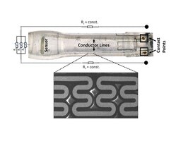
- Flexible electronics
- Micromedicine
- Intelligent implants
- Embedded systems
- 3D micro- and nanostructuring
- Self-organised systems in micro- and nanotechnology
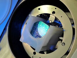
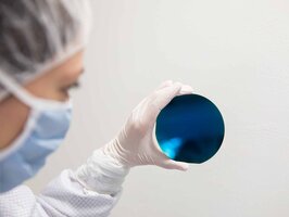
Formerly known as the “micro laboratory”, our lab was one of the first microsystems technology laboratories in Germany, opened in 1984. Since then, innovative technologies have been continuously added to the laboratory's equipment. We operate an extensive silicon technology line and characterisation facility in several clean rooms covering an area of over 300 m². As a member of the Internal link opens in the same window:iMST, we have the opportunity to use the facilities of the Internal link opens in the same window:Rottweil Research Center and to cooperate with other research institutes.
Characterisation
Various devices are available for analyzing microsystems, whereby the FIB-SEM device is particularly noteworthy due to its versatility.
- FIB-SEM: Scanning electron microscope with focused Ga+ ion beam
- Detectors: Inlens (SE and RE), SESI, sTEM, BSE
- With material characterisation: ToF-SIMS, EDX, EBSD
- Structuring using precursors
- FT-IR with microscope
- Optical 3D profiler (laser scanning microscope & white light interferometer)
- Atomic force microscope (AFM)
- Contact profilometer
- Optical layer thickness measurement using ellipsometer and spectrometer
- Capacitance-voltage measurement (4-point method)
- Surface and pore size measurement using physisorption
- Contact angle measurement
- Vibration and distance measurement using laser interferometers and triangulation
- As well as several microscopes and other small devices
Coating processes
There are a wide variety of coating systems that are used for the construction of microsystems:
- Atomic layer deposition (thermal or plasma assisted). The vacuum chamber is integrated in a cluster system with RIE and PECVD
- Vapour deposition of various materials
- Chemical vapour deposition (CVD): PECVD (Si3N4 with controllable voltage, SiC and amorphous Si, SiO2)
- Sputtering system (Pt, Si3N4, Ti, Al/Cu...)
- Microplating: one Fontaine and one rack system
Lithography
Photolithography plays a crucial role in the production of microsystems and is an important structuring technique. There are various photolithographic processes in the laboratory, which are located in a yellow room.
- Grayscale exposure for the creation of 3D structures
- Direct laser exposure for structures up to 600 nm
- In-house production of masks
- Contact exposure / mask aligner
- Alignment accuracy up to 200 nm, IR alignment, front to back alignment
Thermal processes
Etching technology
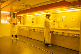
Etching benches © Furtwangen University Silicya Roth & Ribeiro Martins
We have more than 25 different wet chemical etching tanks and several dry etching systems that enable us to structure a wide variety of layers. We have gained extensive experience in the anodization of porous silicon in particular.
- Electrochemical etching: Anodizing systems for porous silicon in hydrofluoric acid solutions
- Dry etching with plasma (RIE suitable for many materials)
- Wet chemical etching (HF, Caro, KOH; Huang A/B...)
Assembly and connection technology
Design, simulation and data analysis
For concept evaluation and analysis of the microsystems we work with:
- FEM simulation using COMSOL Multiphysics®
- Process simulation using IntelliSuite
- Various CAD design programs
- Tomography (of FIB-SEM images) with Dragonfly 3D World
- Mountain SPIP®
Institute management
We are happy to provide information about the research of the IfAG Institute!
Dean of Studies Engineering and Business Management (MSc) (EBM)
Deputy Dean of Studies:
Micromedical Engineering (MSc) (MZT) /
Deputy Dean of Studies Biomedical Engineering (MSc) (BEM)
Smart Systems Master (MSc) (SMA)
Deputy Dean of Studies Technical Physician (MSc) (TP)

![[Translate to English:] Automatisierte Härteprüfanlage](https://www.hs-furtwangen.de/fileadmin/_processed_/c/2/csm_mme_tnm_AutomatisierteHaertepruefanlage_54e1f87d76.jpg)
![[Translate to English:] Ellipsometer](https://www.hs-furtwangen.de/fileadmin/_processed_/1/f/csm_mme_tnm_Ellipsometer_137d349f75.jpg)
![[Translate to English:] FIB-SEM Innenansicht](https://www.hs-furtwangen.de/fileadmin/_processed_/f/b/csm_mme_tnm_FIB-SEMInnenansicht_be5a1c04be.jpg)
![[Translate to English:] FIB-SEM mit ToF-SIMS, EDX, EBSD, Ga+](https://www.hs-furtwangen.de/fileadmin/_processed_/3/3/csm_mme_tnm_FIB-SEMmitToF_bb592749af.jpg)
![[Translate to English:] FT-IR Spekrometer](https://www.hs-furtwangen.de/fileadmin/_processed_/6/b/csm_mme_tnm_FT-IRSpekrometer_c38760d327.jpg)
![[Translate to English:] Laserscanning-Mikroskop](https://www.hs-furtwangen.de/fileadmin/_processed_/1/6/csm_mme_tnm_Laserscanning-Mikroskop_98c706aed5.jpg)
![[Translate to English:] Mikroskope](https://www.hs-furtwangen.de/fileadmin/_processed_/d/7/csm_mme_tnm_Mikroskope_0d1f9d3d81.jpg)
![[Translate to English:] Mikrotopographie mittels Stereo SEM Bilder und Mountains](https://www.hs-furtwangen.de/fileadmin/_processed_/f/c/csm_mme_tnm_MikrotopographieStereoSEM_1ec964c034.jpg)
![[Translate to English:] SEM Bild koloriert](https://www.hs-furtwangen.de/fileadmin/_processed_/c/3/csm_mme_tnm_SEMBildkoloriert_588d9c99c4.jpg)
![[Translate to English:] Weißlichtinterferometer](https://www.hs-furtwangen.de/fileadmin/_processed_/4/a/csm_mme_tnm_Weisslichtinterferometer_7aab77742d.jpg)
![[Translate to English:] ALD-RIE-PECVD-Cluster](https://www.hs-furtwangen.de/fileadmin/_processed_/8/0/csm_mme_tnm_ALD-RIE-PECVD-Cluster_d3b9caaf98.jpg)
![[Translate to English:] Mikro ALD](https://www.hs-furtwangen.de/fileadmin/_processed_/0/9/csm_mme_Mikro03_ALD_c9879db25c_2c6ac0616d.jpg)
![[Translate to English:] Entwicklung Fotoresist](https://www.hs-furtwangen.de/fileadmin/_processed_/8/9/csm_mme_tnm_EntwicklungFotoresist_088a485bba.jpg)
![[Translate to English:] Laserschreiber](https://www.hs-furtwangen.de/fileadmin/_processed_/a/8/csm_mme_tnm_Laserschreiber_c84a9ece47.jpg)
![[Translate to English:] Mikro Mask Aligner](https://www.hs-furtwangen.de/fileadmin/_processed_/d/f/csm_mme_MikroMaskaligner_e541d9312f_201c8fcb47.jpg)
![[Translate to English:] Maskenherstellung](https://www.hs-furtwangen.de/fileadmin/_processed_/0/8/csm_mme_tnm_Maskenherstellung_f8e4ac4ce0.jpg)
![[Translate to English:] Schreibkopf Laser](https://www.hs-furtwangen.de/fileadmin/_processed_/f/4/csm_mme_tnm_Schreibkopf_0da13c1ccf.jpg)
![[Translate to English:] Drahtbonden an einem Mikrofon](https://www.hs-furtwangen.de/fileadmin/_processed_/b/8/csm_mme_tnm_Drahtbonden_c2797797a7.jpg)
![[Translate to English:] Mikro Laserschneider](https://www.hs-furtwangen.de/fileadmin/_processed_/6/c/csm_mme_Mikro_Laserschneider_a5e81fd721_b0884da785.jpg)
![[Translate to English:] CAD Layout](https://www.hs-furtwangen.de/fileadmin/_processed_/6/5/csm_mme_tnm_CADLayout_3b35e3b8f7.jpg)
![[Translate to English:] FEM Simulation eines Miniaturisierten Inchworm aktuator](https://www.hs-furtwangen.de/fileadmin/_processed_/4/f/csm_mme_tnm_Membranverformung_ebd57b9148.jpg)
![[Translate to English:] Mikro Harvester](https://www.hs-furtwangen.de/fileadmin/_processed_/0/6/csm_mme_tnm_MikroHarvester_9046160770.jpg)
![[Translate to English:] SolidWorks-Konstruktion eines Aktor System, inch-worm](https://www.hs-furtwangen.de/fileadmin/_processed_/b/4/csm_mme_tnm_SolidWorks-inch-worm_186e7dee68.jpg)
![[Translate to English:] Wirbelströme Mikrospule](https://www.hs-furtwangen.de/fileadmin/_processed_/0/6/csm_mme_tnm_WirbelstroemeMikrospule_9ccccac288.jpg)