The Institute of Microsystems Technology (iMST) has been researching new microsystems, associated modelling and manufacturing processes and characterisation methods for many years. The iMST is one of the largest research institutes at HFU and its research results are also recognised internationally.
Today, millions of microsystems are used in automobiles (sensors), in communication technology (microphones and high-frequency components, smart phones, micromirrors in projectors, print heads in inkjet printers) and in medical technology (retina implants, cochlear implants). This requires structures in the micrometer range, which are produced using microtechnical processes and combine electronic and non-electronic functions in the smallest of spaces in a single system.
The highly motivated, multidisciplinary team conducts research in numerous cooperation projects with companies, scientific institutions and universities on application-oriented issues in microsystems technology.
Functional coatings
Functional coatings
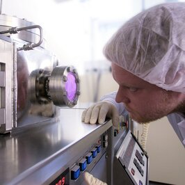
Functional surfaces help to adapt materials to their environment without changing their volume properties. On the one hand, the surface can be adjusted to be hydrophobic/oleophobic or hydrophilic/oleophilic, but the interaction in a physiological environment (biocompatibility) can also be tailored using thin coatings with layer thicknesses in the nanometer to micrometer range. Another field of application is the barrier against diffusion of gases or liquids. This means that thin layers can also be used to protect mechanically flexible components or active implants against harsh environments. A 100% protective effect against corrosion is essential, especially if the electronics to be protected have DC voltage potentials. The miniaturisation of medical products is also increasingly demanding high-voltage-resistant and biocompatible insulating coatings with a low layer thickness.
The homogeneous, defect-free coating of complex geometries is a particular focus of research and development at the institute. In addition to the coating methods, there are also extensive options for validating the homogeneity, defect-free nature and stability of the deposited coatings after exposure to thermal, chemical and cyclical mechanical stress.
Micro- and nanostructuring processes
The ability to specifically produce structures in the micrometer (1 µm = 10-⁶ m) to nanometer (1 nm = 10-⁹ m) size range is one of the core competencies in microsystems technology and therefore also in iMST. Structuring is usually carried out in a two-stage process in which the structures are first created in a photosensitive coating using photolithography and then transferred to the underlying thin film using etching technology ("negative structuring") or molded using electroplating, for example ("additive structuring"). The smallest structures down to 0.6 µm (lateral dimension) and tolerances of around +10% can be produced at the iMST using mask-based photolithography and laser direct writing. Etching techniques for the second structuring step, in which the photoresist structures are transferred to the thin film, include various wet-chemical processes for highly selective etching as well as reactive ion etching (RIE) with high anisotropy for the highest structural quality requirements.
A special field of research at the iMST is the production of quasi 3D microstructures using so-called "grayscale technology", for which three different processes are being investigated at the iMST. Structure heights and depths of typically up to 50 µm can be produced here.
For the nanostructuring of silicon, research is being conducted into the generation of self-organised nanostructures by electrochemical anodisation of silicon (porous silicon). Targeted nanostructuring can be used, for example, to produce multilayers with a precisely adjusted refractive index as optical filter layers in the visible to MIR (mid-infrared) range. These porous layers are also used at the iMST for various sensor principles.
An ns laser (Nd:YAG, wavelength of 1064 nm) is available for the direct structuring of thin films (e.g. 50 µm thick), although this can only be used to produce structures in the size range above 20 µm.
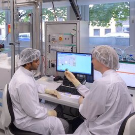
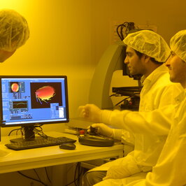
Development of miniaturised sensors and actuators
Miniaturised sensors and actuators are examples of microsystems and are used today by the billions in cars and smart phones. The iMST has many years of expertise in the development of micromechanical sensors and actuators (so-called MEMS sensors and actuators), primarily based on the material silicon. This also includes optical systems that can be used, for example, for focusing, in laser scanners or for filtering light, for which actuator functions are used in each case. In recent years, many research projects at iMST have focused on flexible, polymer-based sensor-actuator systems. The area of application is mostly in medical technology. SOI (silicone on insulator) is usually used as the technology platform.
In addition to the described expertise in the field of micro- and nanostructuring technology, so-called finite element methods are used for the targeted development of sensor and actuator systems, which can be used to simulate very different physical problems and systems. By using this so-called "multiphysics simulation", complex test runs can be largely avoided and sensor and actuator prototypes can be realised in a targeted manner based on specified requirements.
Examples of sensors developed in recent years:
Surface and interface analysis
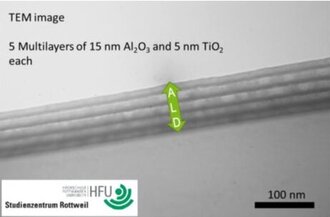
Cross-section preparation of a barrier layer made of aluminum/titanium oxide nanolaminate
Surface and interface analysis at iMST is concerned with examining the surface and layer morphology of a sample, i.e. the structural composition and microstructure of a layer. In addition to roughness and step height, a chemical analysis of the surface and the area close to the surface is also carried out if required. Contamination of the surface, chemical composition of the near-surface area or, for example, wettability as a result of surface activation can be investigated. Cross-section preparations are usually carried out to investigate the layer properties of the near-surface area. In the case of porous materials, for example, the pore size can also be determined in depth. However, cross-section preparations are also used in particular for multilayer coatings (nanolaminates).
The analysis methods used include:
- Light microscopy
- Scanning electron microscopy with energy dispersive X-ray spectroscopy (EDX)
- Transmission electron microscopy with EDX and electron energy loss spectroscopy
- Atomic force microscopy
- Contact angle measurement
- Ellipsometry
- Fourier transform infrared spectrometer
These analysis options can be used to investigate fundamental questions and validate layer properties, particularly for layers with structure sizes in the nanometer or micrometer range. The following image shows a cross-sectional preparation of a barrier layer consisting of an aluminum oxide/titanium oxide nanolaminate, which was produced using atomic layer deposition (ALD). The image was taken under a transmission electron microscope.
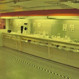
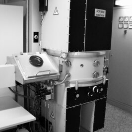
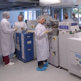
Labs and equipment
The outstanding facilities at the Rottweil Research Center and the Technology Laboratory for Nano and Microsystems in Furtwangen are used at the Institute of Microsystems Technology.
Innovative plasma coating technologies are the central focus at the Rottweil Research Center. A fully developed silicon technology is operated in the technology laboratory for nano and microsystems. This enables the processing of structures down to the nanometer range and the prototypical realisation of micro and nano systems.